IBM outs integrated circuit that’s made from wafer-size graphene, smaller than a grain of salt

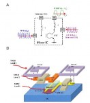
Lest you don’t care what your circuits are made of, listen up: graphene’s the thinnest electrical material, comprising just a single atomic layer. In addition to its electrical, thermal, mechanical, and optical properties, researchers dig it because it has the potential to be less expensive, more energy-efficient, and more compact than your garden-variety silicon. So imagine IBM’s delight when a team of company researchers built the first circuit that fits all the components, including inductors and a graphene transistor, on a single wafer — a setup that consumes less space than a grain of salt. The advantage, scientists say, is better performance than what you’d get from a circuit combining a graphene transistor with external components. In fact, the researchers got the circuit’s broadband frequency mixer to operate at 10GHz , a feat that could have implications for wireless gadgets running the gamut from Bluetooth headsets to RFID tags. That’s all just a layman’s explanation, of course — check out the latest issue of Science for the full paper in all of its technical glory. IBM outs integrated circuit that’s made from wafer-size graphene, smaller than a grain of salt originally appeared on Engadget on Thu, 09 Jun 2011 15:00:00 EDT. Please see our terms for use of feeds . Permalink


Posted by
on June 9, 2011. Filed under
News,
Tech.
You can follow any responses to this entry through the
RSS 2.0.
You can skip to the end and leave a response. Pinging is currently not allowed.

